
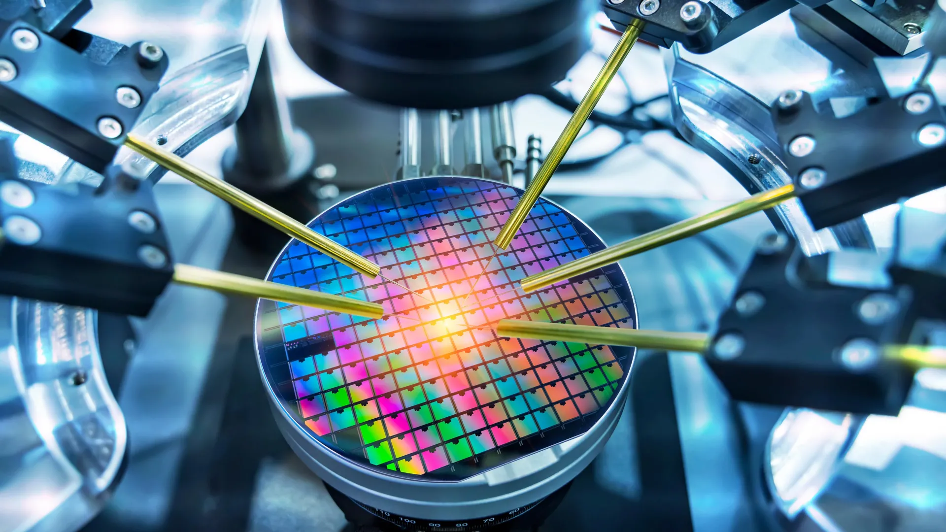
Researchers have used a low-emissions method to harvest hydrogen and graphene from waste plastics. They say it not only solves environmental problems like plastic pollution and greenhouse gas production, but the value of the graphene by-product could offset the costs of producing hydrogen. Hydrogen is used to power vehicles, generate electricity, and heat our homes and businesses. Hydrogen contains more energy per unit of weight than fossil fuels, which is important from an environmental…..Continue reading…
Source: New Atlas
.
Critics:
Efforts to reduce the use of plastics, to promote plastic recycling and to reduce mismanaged plastic waste or plastic pollution have occurred or are ongoing. The first scientific review in the professional academic literature about global plastic pollution in general found that the rational response to the “global threat” would be “reductions in consumption of virgin plastic materials.

Along with internationally coordinated strategies for waste management” – such as banning export of plastic waste unless it leads to better recycling – and describes the state of knowledge about “poorly reversible” impacts which are one of the rationales for its reduction.
Some supermarkets charge their customers for plastic bags, and in some places more efficient reusable or biodegradable materials are being used in place of plastics. Some communities and businesses have put a ban on some commonly used plastic items, such as bottled water and plastic bags. Some non-governmental organizations have launched voluntary plastic reduction schemes like certificates that can be adapted by restaurants to be recognized as eco-friendly among customers.
In January 2019 a “Global Alliance to End Plastic Waste” was created by companies in the plastics industry. The alliance aims to clean the environment from existing waste and increase recycling, but it does not mention reduction in plastic production as one of its targets. Moreover, subsequent reporting has suggested the group is a greenwashing initiative. On 2 March 2022 in Nairobi, representatives of 175 countries pledged to create a legally binding agreement to end plastic pollution.
The agreement should address the full lifecycle of plastic and propose alternatives including reusability. An Intergovernmental Negotiating Committee (INC) that should conceive the agreement by the end of the year 2024 was created. The agreement should facilitate the transition to a circular economy, which will reduce GHG emissions by 25%. Inger Andersen, executive director of UNEP called the decision “a triumph by planet earth over single-use plastics”.
In the lead up to the Assembly, global public opinion on a plastic treaty was surveyed, analysed and reported by The Plastic Free Foundation in partnership with Ipsos and WWF-International. The report identified that nearly 90% of survey participants – over 20,000 adults across 28 countries – believed that having a global plastics treaty will help to effectively address the plastic pollution crisis.
The use of biodegradable plastics has many advantages and disadvantages. Biodegradables are biopolymers that degrade in industrial composters. Biodegradables do not degrade as efficiently in domestic composters, and during this slower process, methane gas may be emitted. There are also other types of degradable materials that are not considered to be biopolymers, because they are oil-based, similar to other conventional plastics.

These plastics are made to be more degradable through the use of different additives, which help them degrade when exposed to UV rays or other physical stressors.Yet biodegradation-promoting additives for polymers have been shown not to significantly increase biodegradation. Although biodegradable and degradable plastics have helped reduce plastic pollution, there are some drawbacks.
One issue concerning both types of plastics is that they do not break down very efficiently in natural environments. There, degradable plastics that are oil-based may break down into smaller fractions, at which point they do not degrade further. A parliamentary committee in the United Kingdom also found that compostable and biodegradable plastics could add to marine pollution because there is a lack of infrastructure to deal with these new types of plastic, as well as a lack of understanding about them on the part of consumers.
For example, these plastics need to be sent to industrial composting facilities to degrade properly, but no adequate system exists to make sure waste reaches these facilities. The committee thus recommended to reduce the amount of plastic used rather than introducing new types of it to the market. Also worth noting is the evolution of new enzymes allowing microorganisms living in polluted locations to digest normal, hard-to-degrade plastic.
An 2021 study looking for homologs of 95 known plastic-degrading enzymes spanning 17 plastic types found a further 30,000 possible enzymes. Despite their apparent ubiquity, there is no current evidence that these novel enzymes are breaking down any meaningful amount of plastic to reduce pollution.

Chair Cardin Introduces Resolution Calling for International Agreement to Reduce Plastic Pollution
.
Labels: #WastePlastics #PlasticPollution #ReduceReuseRecycle #EcoFriendly #SustainableLiving #RecyclingAwareness #PlasticWaste #GreenPlanet #ProtectOurOcean #WasteManagement #EnvironmentalImpact #CircularEconomy #SustainableSolutions #PlasticFreeFuture #ConserveNature #Hydrogene #CleanPlanet #StopPlasticPollution #WasteLessLiveMore #Graphene


Leave a Reply